First silicon · In fab · Live progress
Zero.
The fabric, in silicon.
Zero is a 15.1 mm² system-on-chip that puts the ThermoEdge fabric on one die: a dual RISC-V control plane, in-memory analog compute, five compute primitives, and a single unified persistent memory. It is in fabrication now — not a roadmap slide.
Last updated May 27, 2026
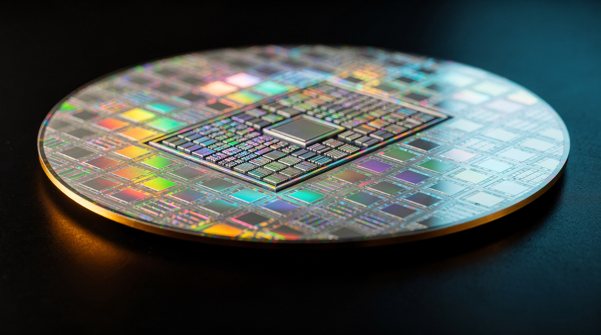
One die
15.1 mm² on SKY130A. The control plane, the reconfigurable mesh, the analog crossbar, the five primitives, and a non-volatile boot ROM all share one 384 KB memory pool and one chiplet bridge to the module companion chip.
Every block is invoked through memory-mapped registers, returns in a fixed number of cycles, and is accounted by the joules it consumes.
What the chip does
Five paradigms, on hardware.
Operations that run forward and backward without erasing information — and so do not pay the kT·ln2 thermodynamic erasure cost that every conventional gate does.
A 1T1R ReRAM crossbar performs matrix-vector multiplication inside the memory cell, by Ohm's law and Kirchhoff summation. The data never moves to a separate compute unit. Non-volatile.
An 8-point FFT and exp / log / tanh / sigmoid arrive as single hardware calls in a fixed cycle count — a whole softmax row or attention activation in one invocation.
A graph-reduction engine does term rewriting and pattern matching in hardware — type checking, symbolic algebra, and theorem-proving kernels without a software interpreter.
An interval-arithmetic coder does lossless compression and channel-adaptive encoding at the link, keeping the chiplet bridge efficient under load.
A domain-level reconfigurable array re-tiles between compute, memory, and extension modes at runtime — the part of the die that adapts to the workload in front of it.
Save and load are pointer dereferences.
Code, working data, and persistent state share one address space. On-die SRAM is a transparent cache over non-volatile memory; a power cycle preserves every byte. No DRAM, no NAND, no file system in the working set. This is Unified Design Architecture in silicon.
uda.thermoedge.ai →Every primitive invocation is metered in joules.
An on-board current sensor brackets the energy integral around each primitive call and ledgers the joules consumed against the workload. Energy is not an estimate after the fact — it is a first-class unit, settled per call.
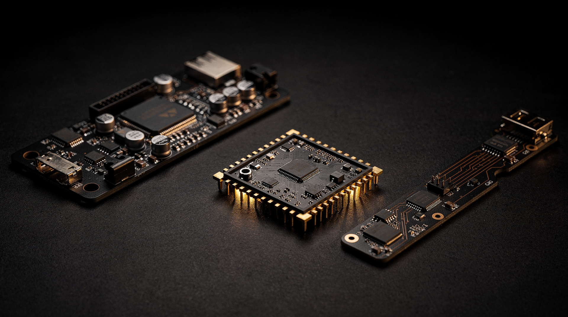
How it ships
Three modules carry the die.
A self-powered connected node — cellular, WiFi, BLE, LoRa, and GNSS over multi-source energy harvesting. Sensing and inference run off harvested power, with no wire and no battery service for the target duty cycles.
Schematic design — radio + harvesting front end
A 25.4 × 25.4 mm castellated module for OEM integration into industrial, edge-AI, and IoT products.
Form factor defined — schematic next
An EDSFF E1.S datacenter module — a CXL 2.0 endpoint the host can offload Joule primitives to, cache-coherently and zero-copy, while its persistent memory appears as a CXL memory tier.
Schematic design — CXL controller locked
Where it stands
Progress, in the open.
This page is the status of record. We update it instead of writing one-off memos.
- ✓ Die in fabrication — ChipFoundry, SKY130A OpenFrame
- ✓ All 26 foundry DRC checks passed
- ✓ Wrapper GDS submitted to fab
- ○ Wafer return — targeted August 2026
- ○ Packaged samples — Q3 2026
- ✓ Chiplet-bridge protocol (GPIF v1.0) frozen at silicon
- ✓ Per-call joule-billing handshake defined in silicon
- ○ SDK in design — Microkit / seL4 on-chip, host runtime on the ThermoEdge stack
- ○ Edge / Embedded / CXL module bring-up follows wafer return
Building on Zero, or backing it?
Sample requests, integration questions, and partnership or investment conversations all start at the same place.